
In the ever-evolving landscape of modern microelectronics, the scaling of CMOS (Complementary Metal-Oxide-Semiconductor) technology emerges as a pivotal force. Discover the profound impact of this relentless scaling on the advancements and possibilities in today’s microelectronic realm.
Technology Scaling and Its Limits
Over the past three decades, CMOS technology scaling has been a primary driver of the electronics industry and has provided a path toward both denser and faster integration [1-5]. The transistors manufactured today are 20 times faster and occupy less than 1% of the area of those built 20 years ago.
The number of devices per chip and the system performance has been improving exponentially over the last two decades. As the channel length is reduced, the performance improves, the power per switching event decreases, and the density improves. But the power density, total circuits per chip, and total chip power consumption has been increasing.
The need for more performance and integration has accelerated the scaling trends in almost every device parameter, such as lithography, effective channel length, gate dielectric thickness, supply voltage, device leakage, etc. Some of these parameters are approaching fundamental limits, and alternatives to the existing material and structures may need to be identified in order to continue scaling.
MOS Scaling Theory
During the early 1970s, both Mead [1] and Dennard [2] noted that the basic MOS transistor structure could be scaled to smaller physical dimensions. The scaling theory developed by Mead and Dennard allows a “photocopy reduction” approach to feature size reduction in CMOS technology, and while the dimensions shrink, scaling theory causes the field strengths in the MOS transistor to remain the same across different process generations.
Thus, the “original” form of scaling theory is constant field scaling. Constant field scaling requires a reduction of the power supply voltage with each technology generation. In the 1980s, CMOS adopted the 5V power supply, which was compatible with the power supply of bipolar TTL logic.
Constant field scaling was replaced with constant voltage scaling, and instead of remaining constant, the fields inside the device increased from generation to generation until the early 1990s, when excessive power dissipation and heating, gate dielectrics TDDB and channel hot carrier aging caused serious problems with the increasing electric field. As a result, constant field scaling was applied to technology scaling in the 1990s.
Moore’s Law
Scaling theory and its practical implementation have been instrumental in bringing about the renowned “Moore’s Law.” This empirical observation states that the number of transistors on integrated circuits doubles approximately every two years, as depicted in Figure 1.

While the exponential growth predicted by Moore’s Law has held true for several decades, it is evident that this trend cannot continue indefinitely. Scientists have grappled with predicting the limitations imposed by material and design constraints, as well as the rate at which further size reduction can be achieved. The future of scaling remains uncertain, challenging researchers to uncover innovative solutions and push the boundaries of microelectronics.
Scaling CMOS Technology to its Limits
There does not seem to be any fundamental physical limitation that would prevent Moore’s Law from characterizing the trends of integrated circuits. However, sustaining this rate of progress is not a straightforward achievement [5]. Figure 2 shows the trends of power supply voltage, threshold voltage, and gate oxide thickness versus channel length for high-performance CMOS logic technologies.
Sub-threshold non-scaling and standby power limitations bound the threshold voltage to a minimum of 0.2 V at the operating temperature. Thus, a significant reduction in performance gains is predicted below 1.5 V due to the fact that the threshold voltage decreases more slowly than the historical trend, leading to more aggressive device designs at higher electric fields.

Trends of power supply voltage Vdd, threshold voltage Vth, and gate oxide thickness tox, versus channel length for CMOS logic technologies.
- improved lithography techniques and non-optical exposure technologies;
- improved transistor design to achieve higher performance with smaller dimensions;
- migration from current bulk CMOS devices to novel materials and structures, including silicon-on-insulator, strained Si and novel dielectric materials;
- circuit sensitivity to soft errors from radiation;
- smaller wiring for on-chip interconnection of the circuits;
- stable circuits;
- more productive design automation tools.
In addition, packaging technology needs to progress at a rate consistent with on- going CMOS technology scaling at sustainable cost/performance levels. This requires advances in I/O density, bandwidth, power distribution, and heat extraction. The system architecture will also be required to maximize the performance gains achieved in advanced CMOS and packaging technologies.
Scaling impact on circuit performance
Transistor scaling is the primary factor in achieving high-performance microprocessors and memories.
Each 30% reduction in CMOS IC technology node scaling has
- reduced the gate delay by 30% allowing an increase in maximum clock frequency of 43%;
- doubled the device density;
- reduced the parasitic capacitance by 30%; and
- reduced energy and active power per transition by 65% and 50%, respectively.
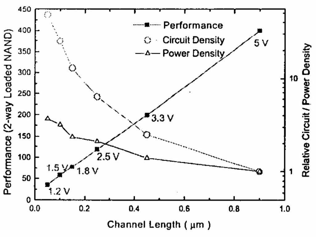
Figure 3 shows CMOS performance, power density and circuit density trends, indicating a linear circuit performance as a result of technology scaling.
References
- C. Mead, “Fundamental limitations in microelectronics – I. MOS technology,” Solid State Electronics, vol. 15, pp. 819–829, 1972.
- R. H. Dennard, F. H. Gaensslen, H-N, Yu, V.I. Rideout, E. Bassous, and A. R. LeBlanc, “Design of ion-implanted MOSFET’s with very small physical dimensions,” IEEE Journal of Solid-State Circuits, SC-9, pp.256–268, 1974.
- H. Iwai, “CMOS Scaling towards its Limits,” IEEE, pp. 31–34, 1998.
- R.D. Isaac, “Reaching the Limits of CMOS Technology,” IEEE, pp. 3, 1998
- S. Borkar, “Design Challenges of Technology Scaling,” IEEE Micro, pp. 23–29, 1999.