A radiation sensor is a dispositive able to detect incoming ionizing particles (such us for example photons,β, gamma or alfa particles) and gives the user information like the energy, the intensity or the position of the radiation.
Among the different approaches to radiation detection, one of the most studied in the last decades is the usage of semiconductor solid-state detectors thanks to the continuous evolution of the semiconductor industries. There are different families of detectors based on semiconductor substrates (Charge Coupled Devices CCD, Silicon Drift Detector SDD, PIN photodiode, etc. ) but the wide diffusion of CMOS technologies in consumer electronics has made very attractive all the implementations of such kind of technology in the field of radiation detectors; the growing diffusion of the CMOS imaging sensors is, for example, the most evident consequence of this fact.
This page is focused on the most common implementation of a radiation sensor in CMOS technologies the Active Pixel Sensor.
The sensing element of Active Pixel Sensors
The main element of Active Pixel Sensors is an inverse-biased photodiode (see Figure 1 and Figure 2). When incoming radiation with energy near or greater than the silicon band gap crosses the depleted region of the p-n junction, some electrons can jump from the valence to the conduction band with the creation of electron-hole pairs; the electric field of the junction separates the generated electron-hole pairs and collects at the electrodes of the photodiode.
The generation of the electron-hole pairs is governed by the approximated relation: n = E / Ebg where n is the number of generated pairs, E is the energy released by the particle and Ebg is the band-gap energy of the silicon. In other words, the radiation generates a photo-current through the photodiode which can be measured directly or as a voltage drop at the ends of the junction. However, the photo-current discharges the photodiode reducing the depleted region and consequentially the sensibility of the detector; there are two techniques to avoid this phenomenon:
- keep continuously the inverse polarization; in this case, the voltage at the photodiode’s ends is always the same and, to detect the radiation, we have to measure the photo-current;
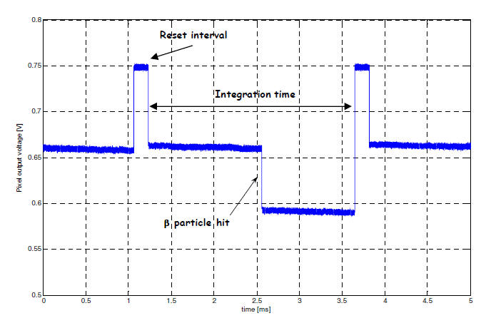
- periodically recharge the photodiode by applying an inverse polarization for a given time and leaving the photodiode floating for the rest of the time. The voltage drop between the beginning and the end of the interval when the junction is left floating will be proportional to the integral of all the charge generated by the radiation during this time; due to this reason such time interval is usually named integration time.
This last approach is the most common in all the sensors arranged as a dense matrix of detectors because it requires less electronics near each photodiode.
To collect the maximum amount of the generated charge, the most common approach is to use a p-substrate where it is realized a small n-well, or a p++ substrate but with an epitaxial p-layer where it is realized the n-well (see Figure 1). In both ways, the n-well collects the electrons while the hole will be lost through the anode placed at the ground potential.
The benefit of this approach is that the mobility of the electrons is higher than the mobility of the holes and the charge collection is faster. The depleted region, in a conventional CMOS sensor, is very narrow due to the lower voltage for which this technology was originally developed; as a consequence, the charge does not reach the cathode for drift but rather for thermal diffusion. In this scenario, it is fundamental to the mean life of carriers in the p-layer.
Such a fact establishes a fundamental difference in the behaviour of the two different technological solutions: in the case of epi-layer the sensitive thickness is limited by the thickness of the p-epi because in the p++ the carriers are affected by faster recombination.

The conventional architecture of Active Pixel Sensors
Figure 2 (a) shows the conventional architecture of a three-transistor APS. The photodiode is connected to the Vrst voltage through the transistor Mrst for inverse polarization; turning off this transistor the photodiode is left floating. After a given integration time, turning on the Msel and imposing a constant current through the transistors Msf and Msel, the voltage at the cathode of the photodiode can be read at the pixel output.

In a pixel sensor, there are a large number of structures shown above, usually arranged in a rectangular matrix (in Figure 2 (b) there is an example of a 3×3 matrix). The reading of each pixel is performed row by row turning on all the Msel of the same row and imposing a current on each column line; at the end of each column can be read the voltage of the corresponding pixel of the selected row. The reset can be distributed row by row or common to all the pixels.

Interaction of Particles with Matter: From Theory to Measurements
Understand the Mysteries of Radiation: Master the Interaction with Matter in a Few Simple Steps
Figure 3 shows a typical output voltage of an APS pixel crossed by a β particle: during the reset interval the pixel is recharged to the reset voltage but, due to the parasitic capacitance between the gate and the source of Mrst, after this operation, there is a little voltage drop. During the integration time, in dark conditions, the voltage remains almost constant unless losses are caused by the leakage current of the photodiode, but, if a particle or photon crosses the pixel, the generated charge causes a fast voltage drop. The signal of each pixel is in general measured as the difference between the initial value, at the beginning of the integration time, and the value at the end.
References
- D. Passeri et al., Characterization of CMOS Active Pixel Sensors for particle detection: beam test of the four sensors RAPS03 stacked system, Nucl. Instr. and Meth. A 617 (2010) 573–575
- D.Passeri et al., Tilted CMOS Active Pixel Sensors for Particle Track Reconstruction, IEEE Nucl. Sci. Symp. Conf. Rec. NSS09 (2009) 1678. July 2006.
- L. Servoli et al. , Use of a standard CMOS imager as position detector for charged particles , Nucl. Instr. and Meth. A 215 (2011) 228-231, 10.1016/j.nuclphysbps.2011.04.016
- D. Biagetti et al., Beam test results for the RAPS03 non-epitaxial CMOS active pixel sensor, Nucl. Instr and Meth A 628 (2011) 230–233